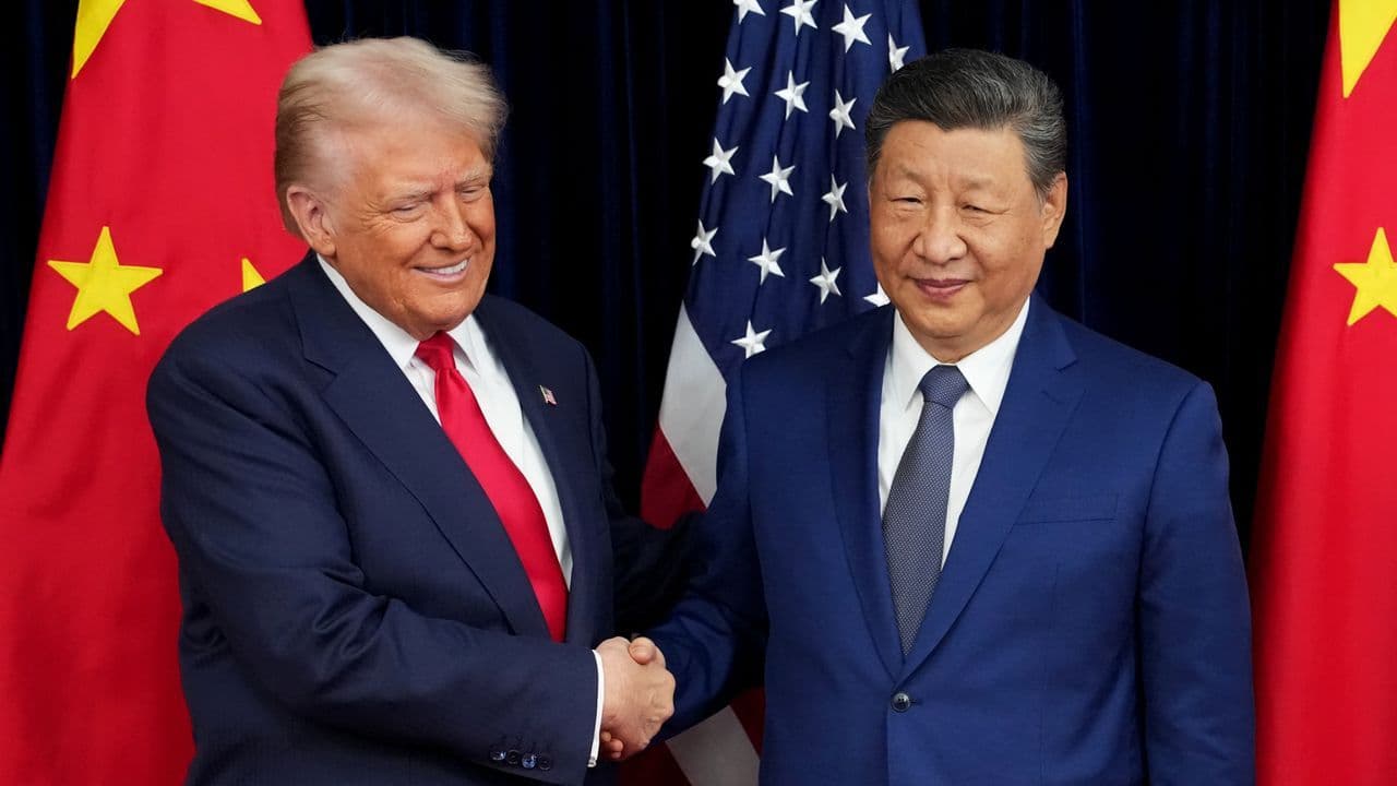
Technical Articles#MicroLED#Display Technology#Data Center#High Brightness#Low Power#Long Lifespan#LED Chip#3D Stacking#Memory Market#DRAM#NAND Flash#Advanced Packaging#Smart Lighting#Thermal Management

LED Companies Accelerate Technological Upgrades to Seize New Opportunities in the Memory Market Requirements: 1. Maintain accurate professional terminology 2. Conform to local business writing conventions 3. Retain all technical details 4. Ensure natural and smooth language Please directly output the translated content.

G
GOPRO LED
··13 min read
LED Companies Accelerate Technological Upgrades to Seize New Opportunities in the Memory Market

Requirements:
1. Maintain accurate professional terminology
2. Conform to local business writing conventions
3. Retain all technical details
4. Ensure natural and smooth language

Please directly output the translated content.

As the global semiconductor industry enters a new "memory super cycle," competition across all links of the supply chain has become increasingly intense. According to the latest report from EE Times, the current memory market is experiencing unprecedented growth. However, at the same time, technical bottlenecks and capacity constraints have placed higher demands on both upstream and downstream segments of the supply chain. In this context, who can break through first in terms of technological iteration and capacity expansion will become the key to determining future market share.

According to industry analysts, the global memory market is expected to grow by more than 15% year-on-year in 2024, with a significant imbalance between supply and demand for DRAM and NAND Flash. Faced with rising raw material costs and complex manufacturing processes, manufacturers are accelerating their deployment of advanced process technologies and new packaging solutions. Particularly in the field of storage chips, technologies such as 3D stacking and high-density integration have become mainstream directions, continuously driving product performance upgrades.

In the field of LED applications, GOPRO LED (Guangpu Electronics) has continuously expanded its applications in display and lighting fields by leveraging its technical advantages in high brightness, low power consumption, and long service life. Its range of high-performance LED modules not only meets the requirements of high-end display equipment for color consistency and stability, but also enhances product reliability through optimized thermal design. Moreover, GOPRO LED's capabilities in smart control and system integration provide downstream customers with more efficient solutions.

Industry experts point out that the rapid expansion of the memory market brings new opportunities for LED companies. With the widespread adoption of data centers, AI computing platforms, and smart terminal devices, the demand for high-performance, low-energy LED products is growing. How to improve production efficiency while ensuring product quality has become a key issue for LED companies to achieve sustainable development.

Overall, the memory super cycle brings not only a surge in market demand, but also a dual test of technology and capacity. For the LED industry, only by continuously innovating and accurately grasping market trends can it maintain a favorable position in the fierce competition.

Source:EE Times

Related Articles

Arm Unveils Its First Silicon-Based CPU Designed for AI Workload Demands, Pioneering a New Direction in High-Performance Computing

Arm Unveils Its First Silicon-Based CPU Designed for AI Workload Demands, Pioneering a New Direction in High-Performance Computing

March 30, 2026

AI-Powered Semiconductor Inspection: Deep Learning Leads a New Era of "Dual-Layer" Technological Competition

In the rapidly evolving LED industry, the integration of artificial intelligence (AI) into semiconductor inspection has become a critical driver for technological innovation. By leveraging deep learning algorithms, manufacturers are now able to achieve higher precision and efficiency in detecting defects at both the wafer and chip levels, ushering in a new era of "dual-layer" technological competition.

The term "dual-layer" refers to the simultaneous enhancement of inspection capabilities at two distinct stages: the initial wafer-level inspection and the subsequent chip-level evaluation. This dual approach ensures that quality control is not only more comprehensive but also more proactive, reducing the likelihood of defective products reaching the market.

Deep learning models, particularly convolutional neural networks (CNNs), have proven highly effective in identifying subtle patterns and anomalies that traditional inspection methods may miss. These models are trained on vast datasets of semiconductor images, enabling them to detect minute defects such as micro-cracks, contamination, and misalignments with exceptional accuracy.

As the demand for high-performance LEDs continues to rise, the competitive landscape is increasingly shaped by the ability to integrate AI-driven inspection technologies. Companies that successfully implement these advanced solutions are gaining a significant edge in terms of product reliability, production efficiency, and overall cost management.

In conclusion, the fusion of AI and semiconductor inspection represents a transformative shift in the LED industry, setting a new benchmark for quality and innovation. The ongoing development of deep learning-based inspection systems will further solidify this trend, driving the industry toward smarter, more efficient manufacturing processes.

AI-Powered Semiconductor Inspection: Deep Learning Leads a New Era of "Dual-Layer" Technological Competition In the rapidly evolving LED industry, the integration of artificial intelligence (AI) into semiconductor inspection has become a critical driver for technological innovation. By leveraging deep learning algorithms, manufacturers are now able to achieve higher precision and efficiency in detecting defects at both the wafer and chip levels, ushering in a new era of "dual-layer" technological competition. The term "dual-layer" refers to the simultaneous enhancement of inspection capabilities at two distinct stages: the initial wafer-level inspection and the subsequent chip-level evaluation. This dual approach ensures that quality control is not only more comprehensive but also more proactive, reducing the likelihood of defective products reaching the market. Deep learning models, particularly convolutional neural networks (CNNs), have proven highly effective in identifying subtle patterns and anomalies that traditional inspection methods may miss. These models are trained on vast datasets of semiconductor images, enabling them to detect minute defects such as micro-cracks, contamination, and misalignments with exceptional accuracy. As the demand for high-performance LEDs continues to rise, the competitive landscape is increasingly shaped by the ability to integrate AI-driven inspection technologies. Companies that successfully implement these advanced solutions are gaining a significant edge in terms of product reliability, production efficiency, and overall cost management. In conclusion, the fusion of AI and semiconductor inspection represents a transformative shift in the LED industry, setting a new benchmark for quality and innovation. The ongoing development of deep learning-based inspection systems will further solidify this trend, driving the industry toward smarter, more efficient manufacturing processes.

March 29, 2026