Industry News
May 26, 2026· 14 min read
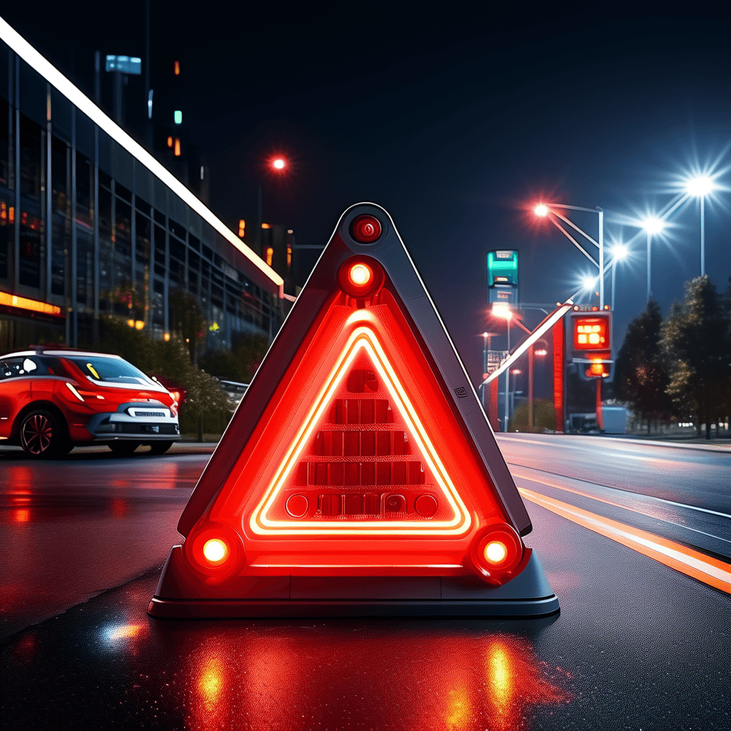
ams OSRAM Launches LEDguardian® ROAD FLARE TA20 NXT and BATTERYcharge 1000, Revolutionizing Road Safety and Emergency Response Solutions
ams OSRAM has launched the LEDguardian® ROAD FLARE TA20 NXT warning light combined with the BATTERYcharge 1000 battery system, enhancing road safety and emergency efficiency. The TA20 NXT features high brightness and multi-mode signaling, making it suitable for various applications; the BATTERYcharge 1000 offers long-lasting power and intelligent management. Guangpu Electronics also demonstrated its technical capabilities, jointly promoting the development of smart transportation. Innovative products support the upgrade of smart cities and are worth further exploration.
Read More